24GHz LNA design
So, here are my thoughts on an LNA design for 24 GHz, inpired by Ron Schiltmans DU3T design, I thought I would try something similar.
The basic concept is a waveguide input, 2 stage desgin for 24GHz, with a CE3520K3 FET on the input, and a MMIC amplifier as the second stage. For the second stage I plan to use an HMC341 I will include my calculations and assumptions for the design, if you can spot an error in my thoughts, I would be of course, delighted to hear from you!
The circuitry on the left is a simple 3.3V regulator, feeding a ICL7660 negative voltage generator. The 3.3V is used to feed power to the MMIC amplifier and the input FET. A simple P type FET prevents power being supplied to the front end FET before the negative voltage is present.

The CE3520K3 was selected as it is pretty much the only real option easily obtainable from Mouser. I'd like to give you a better answer based on cost and performance, selection of matching parameters etc, but basically, it comes down to availability.
The matching data came from the datasheet for the input FET, which is handily provided by the manufacturer, complete with optimum reflection coefficients for best noise at 24GHz.

We can see that best noise figure is obtained with a reflection coefficent of 0.213/ -50.857 degrees presented to the input of the FET. Converting that reflection coefficient to a complex impedance we get 61.47 -j 21.27 Our goal in matching is to provide a circuit that transforms the (hopefully) 50 ohm input impedance to this complex impedance. The tool of choice for this is SimSmith, the plot and matching circuit is shown below.

We can see that a length of 37 degrees of 71 Ohms of microstrip will perform the desired transformation. The width of the 50 Ohm and 71 Ohm strips was obtained from the Roger PCB calculator, for RO4003C in 0.508mm thickness. The software also provides the velocity factor of 0.604 which is put back into SimSmith which produces a lenght of 0.78mm for the matching section. These elements are then inserted on the PCB directly before the input to the FET.
Using the usual equation for the output match:
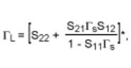
I wrote a small program in Perl to perform the calculation. Feeding in the input reflection coefficient from above, and the S parameters from the datasheet:
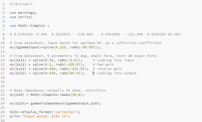
I ran the program and got the output impedance of the FET first stage as follows:

I then fed the output impedance of 34.05 -j 37.47 ohms back into SimSmith and selected appropriate stripline elements to transform this to 50 ohms:

The two matching elements of 30 degrees of 75 Ohms and 90 degrees of 36 Ohms were selected and these were added to the ouput of the FET to transform the impedance to the 50 Ohms of the microstrip and the input of the second stage.
I did not perform any analysis of stability criteria, I have seen it done, but as yet, it is above my pay grade.
The second stage has internal matching and isolation capacitors, so no additional input DC block is needed. 0402 sized resistors and bypass C's were selected, as these are about as small as I can reliably place by hand.
The input "window" is based on RG42 waveguide and flange sizing, the probe length is selected at 2.41mm and 1.27mm wide, this is from W1GHZ's SMA transition data, which gives a probe diameter of 1.27mm and a length of 2.41mm ... handily, our 50 Ohm track is very close to 1.27mm so no transition was needed ...
The "backshort" will be machined into the aluminium casing for this PCB, 2.49mm is specified .. I'm going to place the board in the aluminium mount with the probe on the "short" side, and the open waveguide side seeing just the PTFE substrate. This should allow me to machine a 2.49mm deep section without having to take into account the velocity factor of the PTFE substrate. If the board is mounted with the probe nearest the open side, the RF has to pass theough the substrate to get to the "short", so an allowance would have to be made for the velocity factor of the PTFE.
Finally, we have the output filter and here I have to confess to what can only be described as guesswork. Much staring at similar filters, poking around in some 24GHz transverter modules with a set of vernier calipers and similar foolish attempts were made ... in the end, I have no clue if it is close or not. The "plan" is to obtain some RO4003C in the appropriate thickness and attempt to photo etch a filter and make a measurement with my signal generator and spectrum analyzer before buying 10 boards from a board house.
The basic layout is shown below:

Boards in RO4003C are not cheap, 10 boards will be around $350 which is "significant" when you have no real clue if they will work! As a shoddy workaround, and just to check the mecahnics of it and any stupid "DC" type mistakes, I'll order a few boards in FR4, which naturally will be miles of in RF terms but will serve to check the basic board for errors before comitting to having some made in RO4003C. I may populate a board in FR4, just for fun ... well, for some values of fun anyway!
Datasheets:
Software:
Rogers MWI2019 (requires login)
Github:
https://github.com/rszemeti/24GHz-VLNA

Comments
Post a Comment